LearnTronics
FJD Six-String Piezo Guitar Electronics
This project documents the redesign of an onboard guitar electronics system built around six individual piezo string pickups. Each string receives its own high-input- impedance buffer and level control before the six channels are summed, while an additional µ-Amp stage provides a separately switchable processing path. The design was developed as both an electrical restoration/redesign project and a practical exercise in turning a working schematic into a compact, serviceable printed circuit board.
Project overview
Design goals
- Preserve six separate piezo pickup channels, one for each guitar string.
- Use a very high input impedance so the raw piezo elements are not heavily loaded.
- Retain individual string-level controls before the channels are summed.
- Keep the pots, switches, DIN connector and audio jack off the PCB and hard-wire them where that produces a cleaner mechanical installation.
- Use conventional through-hole parts wherever practical so the board remains easy to assemble, modify and troubleshoot.
- Retain the separate µ-Amp stage while integrating it cleanly with the larger guitar circuit.
- Produce a PCB small enough to fit behind the original control plate without forcing the board to carry the mechanical load of the controls.
Mechanical starting point
The original guitar used a metal control plate mounted beneath the guitar top/bridge. Six string pots occupied a curved row, with separate volume/tone controls toward the right. The plate was traced on 1/4-inch graph paper so the existing geometry could be used as a mechanical reference.
An early idea was to solder the pot leads directly into the PCB. That was abandoned after measuring only about 0.100 inch of clearance between the pot face and its leads. The revised approach leaves the controls on the plate and uses short hard-wired leads to individual PCB solder pads.
Signal path
Six piezo pickup inputs
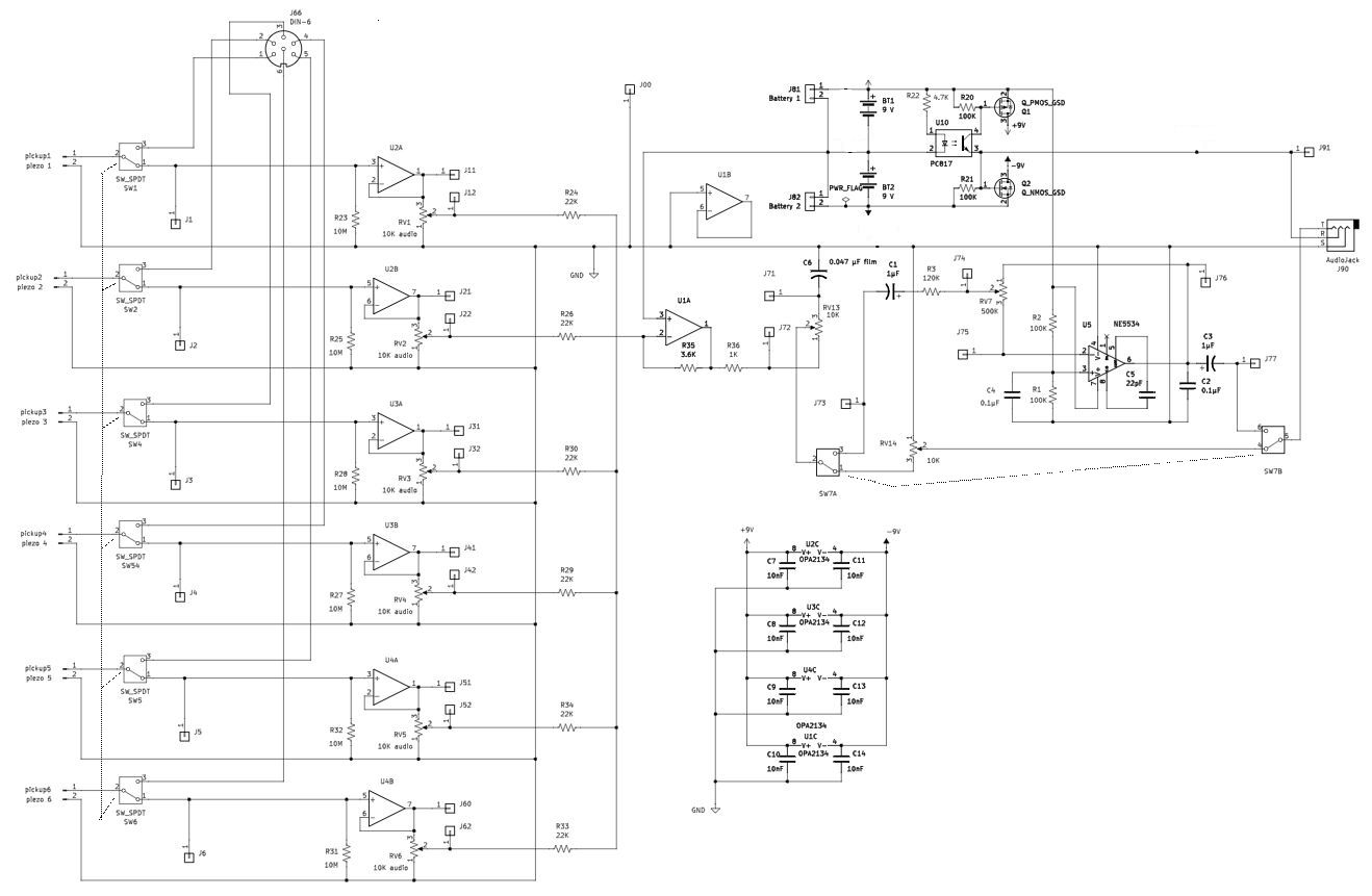
Each string has its own piezo element. The pickup hot lead first goes to its off-board selector switch. One switch path is routed directly off-board to the DIN-6 connector, while the processed path enters the PCB through a single solder pad and feeds its corresponding preamplifier channel.
The piezo inputs use 10 MΩ bias/input resistors. This high impedance is important because a piezo element behaves as a high-impedance capacitive source; loading it heavily would reduce low-frequency response and produce a thinner sound.
OPA2134 string buffers
The six string channels are buffered with OPA2134 dual JFET-input audio op amps in through-hole DIP-8 packages. The design originally considered the OPA1656, but the OPA1656 is not available as a conventional DIP part. The OPA2134PA was selected so the board could remain predominantly through-hole while still presenting a very high input impedance to the piezo pickups.
Four physical OPA2134 packages are used across the complete circuit. Each package has local 10 nF supply-bypass capacitors from +9 V to ground and from -9 V to ground, placed close to the IC power pins on the PCB.
Individual string level controls
Each buffered string drives an off-board 10 kΩ string pot. Only two wires from each pot need to return to the PCB: the buffered signal going out to the pot and the wiper signal returning to the summing network. The ground terminals of the six pots are daisy-chained off-board and return to the PCB through one common ground point.
Summing and following stages
The six wiper signals return through individual 22 kΩ summing resistors. This keeps the channels isolated from one another while combining them for the following amplifier and master-control stages. The layout keeps the repeated channel structure recognizable so a future service technician can follow one string path from input to pot to summing node.
µ-Amp section
The µ-Amp portion uses an NE5534 and intentionally operates from a single +9 V supply referenced to ground, rather than from the full ±9 V rails used by the main audio path. Two 100 kΩ resistors create an approximately 4.5 V mid-rail reference for the NE5534 signal path. Input and output coupling capacitors keep that internal DC bias from being passed to the surrounding circuitry.
During the schematic review the NE5534 compensation capacitor was corrected to 22 pF, and the input coupling capacitor orientation/type was reviewed so the single-supply biasing would be handled correctly.
Power system
Two 9 V batteries are connected in series. Their midpoint is the circuit's 0 V / ground reference, giving the main preamplifier a +9 V rail and a -9 V rail. The µ-Amp section uses only +9 V and ground.
| Node | Function |
|---|---|
| B1+9 | Raw positive battery rail before the positive-side MOSFET switch. |
| +9V | Switched positive rail used by the main circuitry and the single-supply µ-Amp. |
| GND / 0 V | Midpoint between the two 9 V batteries and the audio reference ground. |
| B2-9 | Raw negative battery rail before the negative-side MOSFET switch. |
| -9V | Switched negative rail used by the split-supply audio stages. |
A PC817 optocoupler and complementary MOSFET switching section are used in the supply control arrangement. An important schematic/PCB cleanup step was giving the raw battery nets different names from the switched +9 V and -9 V nets. Without that distinction, KiCad treated both sides of a MOSFET as the same electrical net and produced confusing routing/DRC behavior.
PCB design
Through-hole construction
The design intentionally favors conventional axial resistors, radial capacitors, DIP op amps, a DIP optocoupler and leaded transistor/MOSFET packages. Off-board controls use individual plated-through solder pads rather than plug-in connectors.
This choice makes the board easier to hand-solder and repair, and it avoids forcing the spacing of the PCB to match the physical spacing of the guitar's pots and switches.
Routing approach
The board is treated as a two-layer design, with most signal routing kept orderly on one side and the second side available for ground/return routing and unavoidable crossings. The normal trace width was set to 1.0 mm, matching the earlier µ-Amp board and providing generous copper for this low-current audio circuit.
Large external solder pads are kept near board edges. Repeated pickup channels are grouped in a recognizable pattern, while the power-switching circuitry and µ-Amp occupy their own areas away from the very high-impedance piezo inputs.
3D component representation
The KiCad VRML export was further refined so the axial resistors use value-specific models with visible four-band color codes. The present model includes 1 kΩ, 3.6 kΩ, 4.7 kΩ, 22 kΩ, 100 kΩ, 120 kΩ and 10 MΩ resistor models, each with a gold 5% tolerance band. This makes the interactive model more useful as an assembly and teaching reference rather than merely a mechanical preview.
Development process
- Preserve the original mechanical idea. The existing guitar control plate was photographed and traced on 1/4-inch graph paper to establish the pot positions, pickup-lead entry points and available space.
- Separate mechanical controls from the PCB. Direct pot-to-board mounting was considered, but the approximately 0.100-inch pot-lead clearance made it impractical. Pots, switches and jacks therefore remain mechanically mounted off-board.
- Simplify external wiring. Every off-board component connection was reviewed individually. A PCB solder pad is retained only where a wire actually has to enter or leave the board. Connections that simply run from one off-board component to another are wired directly.
- Keep the piezo inputs high impedance. The six pickup inputs use 10 MΩ resistors before the FET-input op-amp stages.
- Change the op-amp package strategy. The OPA1656 was replaced with the DIP-8 OPA2134PA so the board could remain a practical through-hole build.
- Review the µ-Amp independently. The NE5534 stage was confirmed as a +9 V-to-ground single-supply stage with a 4.5 V bias reference. Its compensation capacitor and coupling details were corrected during review.
- Add local supply bypassing. Eight 10 nF capacitors were added around the four OPA2134 packages, one from each supply rail to ground for every physical dual op amp.
- Clean the schematic for PCB transfer. Generic multi-pin connectors were replaced by individual solder-pad symbols where that better represented the actual installation. Descriptive connector-value text was hidden in bulk to make the schematic easier to read.
- Resolve raw versus switched power nets. The battery-side nets were renamed B1+9 and B2-9, while +9V and -9V were reserved for the switched rails after Q1 and Q2. This removed ambiguous DRC behavior and made the power topology explicit.
- Place first, route second. Components were initially spread outside the board outline, grouped by function, and then moved into the board in logical blocks. Routing was delayed until the repeated channels, summing network, µ-Amp and power section were easy to recognize.
- Verify continuously. ERC and DRC were rerun after major changes so accidental floating nets, duplicate power flags, layer-transition mistakes and tiny track fragments could be found before the board became difficult to revise.
- Finish with a useful 3D model. The board was exported to VRML, the component models were collected into one project directory, and resistor color bands were added so the model corresponds more closely to the real through-hole assembly.
Schematic
Interactive 3D board
The viewer below loads the KiCad VRML export from
vrml/fjd_guitar/fjd-guitar01.wrl. Component shape files are expected in the
same vrml/fjd_guitar/ directory. The page resolves the KiCad Inline model
references before handing the complete model to the viewer.
Installation notes
- The six pickup selectors, string pots, master controls, DIN-6 connector and output jack are off-board components.
- Use short, tidy leads between the control plate and the PCB; keep the six high-impedance pickup input runs away from power-switching wiring where practical.
- The six string-pot ground terminals may be daisy-chained off-board and returned to the board at the designated common ground pad.
- Observe the split-supply wiring carefully: the two-battery midpoint is 0 V/GND, not the negative rail.
- The µ-Amp uses +9 V and GND only; the main OPA2134 circuitry uses the ±9 V split supply.
- Verify all off-board switch and pot terminal numbers against the physical parts before final soldering.